I have been getting back into hardware again. It is so frustrating its fun.
I've noticed some pain-points in the the process, and developed a tool with a friend that is quite useful.
I believe there are two valuable aspects to PCB design that can be automated with:
- Part sourcing
- Semantic Rule Check (SRC)
traces is four pieces that form one loop: the mcp grounds an LLM in real supplier data so it can actually find parts, the KiCad extension uses that to populate your schematic so it becomes the source of truth, a tuned agent makes the sourcing cheap and fast enough to feel instant, and the SRC reads the now-complete schematic to catch the semantic bugs ERC can't. Source the parts → fill the schematic → check the schematic.
Part Sourcing
LLMs are horrible at finding parts for a project, mostly because all the part information are hosted on a few distributor sites that these labs weren't able to train on.
Let us say there are three main suppliers for electronic parts:
- Digikey
- Mouser
- LCSC
The idea: ground a LLM query with real data from the supplier site.
This is the traces mcp.
It is very simple. You connect your LLM to the mcp, and ask it for a part.
Ok very useful. Use it- its open-source.
Wouldn't it be nice if it could just populate the information so you can use the schematic as the source of truth so you didn't have to run around copy/pasting data...
KiCad Extension
Imagine if your schematic was fully reconciled:
- each symbol has a real part associated with it
- each part has a supplier associated with it
- each part has a qty available
- each part has a datasheet downloaded locally
- each part has a price
We built a kicad extension where you can do this automatically while still being in your eda.
If you don't have all the information filled, don't worry. Press Source and it will go through, one by one, until your schematic is complete!
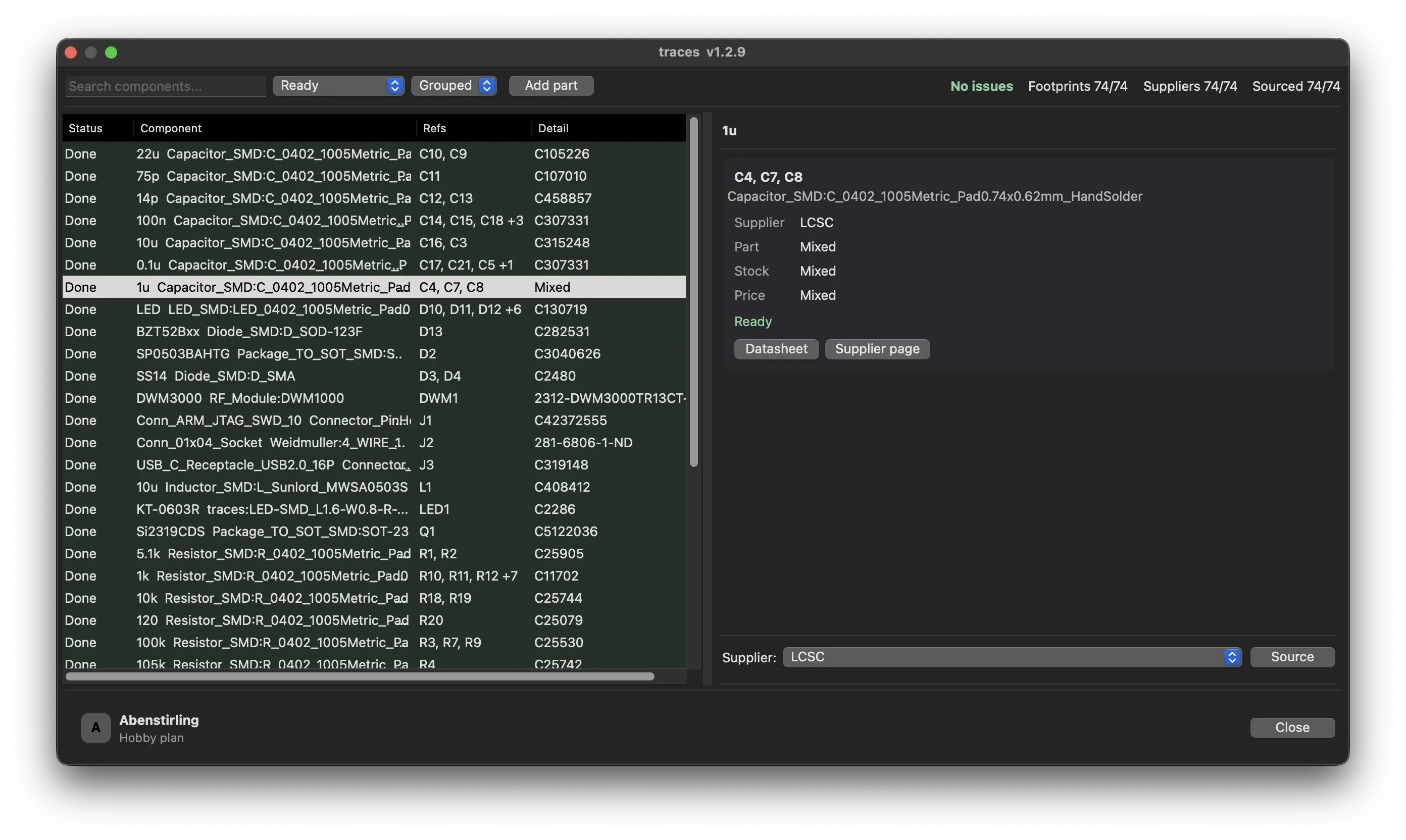
But you might have noticed, there needs to be a LLM to run the query in order to fill the proper information?
traces agent / eval
That Source button has to call something. The first version handed the request to a general-purpose Claude agent and let it drive the supplier APIs.
It worked, but it was ~$0.10 per part. That doesn't scale when a board has 80 parts.
Oh, and it could take up to a minute per part. Horrid. I don't have to have taste to know that is trash UX — if anything loads for more than 5 seconds my intuition is that it's borked.
So we treated model choice as a benchmark instead of a default. The sourcing work is small and well-defined — take a natural-language request, call a supplier tool, return a ranked in-stock part — so a frontier model is overkill. Everything runs behind one OpenAI-compatible API, so the same agent races a local model and a handful of OpenRouter models on the exact same workload:
# bench.py — "ollama/" routes to the local model; everything else is OpenRouter
MODELS = [
    {"id": "ollama/gemma4",                "price": (0.00, 0.00)},   # local, free
    {"id": "google/gemini-3.5-flash",      "price": (1.50, 9.00)},
    {"id": "openai/gpt-5-mini",            "price": (0.25, 2.00)},
    {"id": "anthropic/claude-haiku-4.5",   "price": (1.00, 5.00)},
    {"id": "google/gemini-3.1-flash-lite", "price": (0.25, 1.50)},   # what the extension ships
    {"id": "qwen/qwen3-235b-a22b-2507",    "price": (0.09, 0.10)},   # one Chinese model
]
The things we cared about, in order: accuracy, then speed, then price. Each model runs the same three JLCPCB searches — a 100nF X7R 0402, a 10k 1% 0603, and a low-Rds N-channel MOSFET in SOT-23 — three trials each, 54 sourcing calls in total. JLCPCB/LCSC needs no supplier key, so the only cost is the LLM itself. A run "passes" if the winning part matches the request on keywords and footprint, and models are ranked accuracy → median latency → avg cost.
Our results — 6 models × 3 cases × 3 trials:
| Model | Accuracy | Median speed | Avg $/run |
|---|---|---|---|
google/gemini-3.1-flash-lite (shipped default) | 100% | 5.6s | $0.00059 |
anthropic/claude-haiku-4.5 | 100% | 7.4s | $0.00394 |
qwen/qwen3-235b-a22b-2507 | 100% | 8.0s | $0.00018 |
openai/gpt-5-mini | 100% | 20.9s | $0.00240 |
ollama/gemma4 (local) | 100% | 44.7s | $0.00 |
google/gemini-3.5-flash | 44% | 18.8s | $0.00796 |
A few takeaways. The shipped default (gemini-3.1-flash-lite) is the fastest and the most accurate cloud option — the cheap Flash model wins outright. qwen3-235b is nearly as good for ~3× less. The local gemma4 matches on accuracy at literally $0, just ~8× slower — so you can run the whole thing offline with no key at all. And bigger isn't better: gemini-3.5-flash, the priciest model here, was the only one to whiff accuracy.
Net effect: swapping a general-purpose agent for a benchmarked Flash-class model took us from $0.10 and up-to-a-minute per part down to **$0.0006 and under six seconds** — roughly two orders of magnitude cheaper and ~10× faster.
Semantic Rule Check (SRC)
You already run a Design Rule Check (DRC) and Electrical Rule Check (ERC). Both are mechanical: spacing, connectivity, unconnected pins. Neither one reads your design.
I would like to propose a third: the Semantic Rule Check (SRC) — the class of bugs that pass DRC and ERC clean but are still wrong.
LLMs are good at language, so why not just have it find
- rotated a usb-c connector 180* and now the
d+is connected to thed-
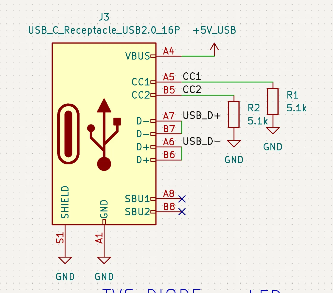
- you change a netlist label from
CAN_RXDtoCAN_RXand don't update all instances - check the rating of the passives for power-related things
Ok those are basic. Imagine if the SRC could read the full schematic in context and flag the weird stuff that only becomes obvious when you understand what the circuit is supposed to do:
- flag a motor driver whose current limit is below the motor's stall current
- catch an IMU placed far from the mechanical center when the design assumes clean motion data
- notice a battery charger configured for the wrong cell chemistry or charge current
- warn when an I2C pullup is missing, duplicated too many times, or tied to the wrong voltage rail
Why now?
- KiCad is becoming widely adopted as a free and open-source EDA that is super capable
- It is a local program with a CLI, and its files are just plain text
- You can use an agent like Claude Code or Codex to actually make the changes once they are detected!
Looking Forward
"Automating electrical engineering" would be the natural progression of these ideas.
Economically, this is a juicy opportunity, and the value shows up in two places.
The tools are expensive. A seat of Altium runs ~$4k–$10k/yr; Siemens (Xpedition / Capital) is enterprise-quote territory north of that. The market already pays a lot for software that helps engineers not make mistakes — and none of it reads the design the way an LLM can.
The mistakes are more expensive than the tools. The real cost isn't the license, it's the respin. Walk one through:
- A semantic bug — a flipped USB-C connector, an underrated cap on a power rail — passes DRC and ERC clean and ships.
- You catch it on the bench. Now you eat a new fab + assembly run and the lead time that comes with it: call it ~2–4 weeks of slip plus ~10–20 hours of engineering time to diagnose, fix, and re-review at $100/hr.
- If it slipped into a production batch instead — say 1,000 boards at ~$100 of raw material each — that's up to $100k of inventory at risk over a single net-name typo.
So the bet is simple: an SRC that runs in seconds against a fully-populated schematic is cheap insurance against a five-figure mistake. That's the whole pitch.
Electrical engineers are smart, and their jobs are complicated.
To list a few of the main roles of their jobs:
- supply chain management
- update / create PCB designs
- physically testing
The implications of a tool that ensures accuracy of PCB design likely means that there will be a consolidation of chips, biasing on ones that:
- have accessible information (datasheet, footprint, availability)
- have good data about them (i.e. ones on the internet that people use)
I am excited for the future of electronic design, and hope traces lays a foundation for what it might look like.